(China (Mainland))

Product Summary
Xilinx introduces the high-density QPro? XQ17V16 series<br />
QML configuration PROM which provide an easy-to-use,<br />
cost-effective method for storing large Xilinx FPGA configuration<br />
bitstreams. The XQ17V16 is a 3.3V device with a<br />
storage capacity of 16 Mb and can operate in either a serial<br />
or byte wide mode. See Figure 1 for a simplified block diagram<br />
of the XQ17V16 device architecture.<br />
When the FPGA is in Master Serial mode, it generates a<br />
configuration clock that drives the PROM. A short access<br />
time after the rising clock edge, data appears on the PROM<br />
DATA output pin that is connected to the FPGA DIN pin. The<br />
FPGA generates the appropriate number of clock pulses to<br />
complete the configuration. Once configured, it disables the<br />
PROM. When the FPGA is in Slave Serial mode, the PROM<br />
and the FPGA must both be clocked by an incoming signal.<br />
When the FPGA is in Master SelectMAP mode, it generates<br />
a configuration clock that drives the PROM and the FPGA.<br />
After the rising CCLK edge, data are available on the<br />
PROMs DATA (D0-D7) pins. The data will be clocked into<br />
the FPGA on the following rising edge of the CCLK. When<br />
the FPGA is in Slave SelectMAP mode, the PROM and the<br />
FPGA must both be clocked by an incoming signal. A<br />
free-running oscillator may be used to drive CCLK. See<br />
Figure 2.<br />
Multiple devices can be concatenated by using the CEO<br />
output to drive the CE input of the following device. The<br />
clock inputs and the DATA outputs of all PROMs in this<br />
chain are interconnected. All devices are compatible and<br />
can be cascaded with other members of the family.<br />
For device programming, either the Xilinx Alliance or Foundation<br />
series development system compiles the FPGA<br />
design file into a standard Hex format, which is then transferred<br />
to most commercial PROM programmers.
Features
? 16Mbit storage capacity<br />
? Guaranteed operation over full military temperature<br />
range: –55° C to +125°C<br />
? One-time programmable (OTP) read-only memory<br />
designed to store configuration bitstreams of Xilinx<br />
FPGA devices<br />
? Dual configuration modes<br />
- Serial configuration (up to 33 Mb/s)<br />
- Parallel (up to 264 Mb/s at 33 MHz)<br />
? Simple interface to Xilinx QPro FPGAs<br />
? Cascadable for storing longer or multiple bitstreams<br />
? Programmable reset polarity (active High or active<br />
Low) for compatibility with different FPGA solutions<br />
? Low-power CMOS Floating Gate process<br />
? 3.3V supply voltage<br />
? Available in compact plastic VQ44 and ceramic CC44<br />
packages<br />
? Programming support by leading programmer<br />
manufacturers.<br />
? Design support using the Xilinx Alliance and<br />
Foundation series software packages.<br />
? Guaranteed 20 year life data retention
| Image | Part No | Mfg | Description |  |
Pricing (USD) |
Quantity | ||||||
|---|---|---|---|---|---|---|---|---|---|---|---|---|
 |
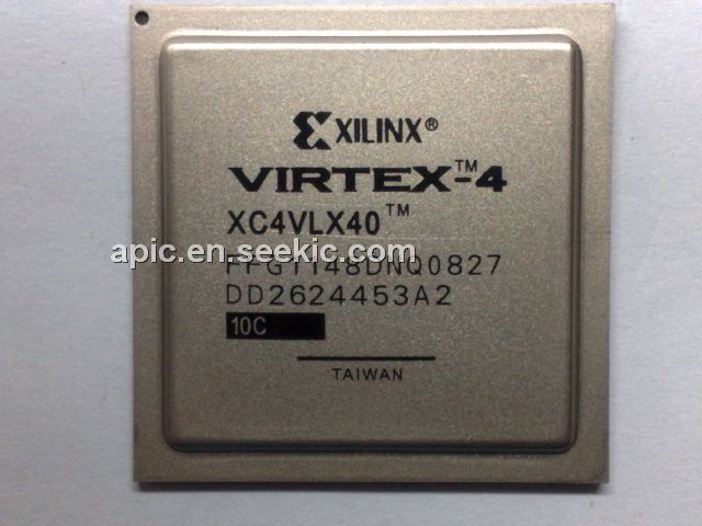
 XC4VLX40-10FFG1148C |
|
IC FPGA VIRTEX-4 40K 1148-FBGA |
Data Sheet |
|
|
||||||
| Image | Part No | Mfg | Description | |
Pricing (USD) |
Quantity | ||||||
 |
XC4VFX100-10FF1152I |
|
IC FPGA VIRTEX-4FX 1152FFBGA |
Data Sheet |
|
|
||||||
|
XC4VFX100-10FF1517I |
|
IC FPGA VIRTEX-4FX 1517FFBGA |
Data Sheet |
|
|
||||||
|
XC4VFX100-10FFG1152C |
|
IC FPGA VIRTEX-4FX 100K 1152FBGA |
Data Sheet |
|
|
||||||
|
XC4VFX100-10FFG1152I |
|
IC FPGA VIRTEX-4FX 100K 1152FBGA |
Data Sheet |
|
|
||||||
|
XC4VFX100-10FFG1517C |
|
IC FPGA VIRTEX-4FX 100K 1517FBGA |
Data Sheet |
|
|
||||||
|
XC4VFX100-10FFG1517I |
|
IC FPGA VIRTEX-4FX 100K 1517FBGA |
Data Sheet |
|
|
||||||